SMIC, the largest contract maker of semiconductors in China, announced this month that it would start commercial production of chips using its 14 nm FinFET manufacturing technology by the end of the year. This is the first FinFET manufacturing line in China, making it a notable development for a country that already houses a significant number of fabs, as the world's leading-edge manufacturers never installed FinFET technology in China for geopolitical and IP reasons. SMIC in turn seems to expect a rather rapid ramp of its 14 nm node, as it anticipates the new manufacturing line will meaningfully contribute to its revenue before the end of the year.
According to SMIC, their 14 nm FinFET manufacturing technology was developed entirely in-house and is expected to significantly increase transistor density, increase performance, and lower power consumption of chips when compared to devices made using the company’s 28 nm process that relies on planar transistors. Earlier this year it was expected that SMIC would start production of 14 nm chips already in the first half of 2019, so the firm seems to be a little behind the schedule. Nonetheless, an in-house FinFET process technology is quite a breakthrough for a relatively small company that puts it into a club with just five other foundries with FinFET technologies.
One interesting thing that SMIC said about its 14 nm FinFET volume ramp is that it expects the process to have a significant revenue contribution already by the end of the year. Meanwhile, keeping in mind that right now SMIC only has two relatively small 300-mm HVM fabs (which are currently used for 28 nm – 65 nm nodes) that are heavily utilized generating 40 ~ 49% of the company’s revenue (in Q1/Q2 2019), it is difficult to imagine SMIC making loads of 14 nm chips in 2019.
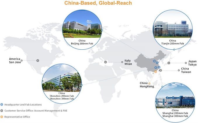
| Overview of SMIC's Fabs |
| Process Technologies | Capacity
Wafer Starts per Month | Location |
| BJ | 200mm | 90 nm - 150 nm | 50,000 | Beijing, China |
| 300mm | 28 nm - 65 nm | 35,000 |
| SH | 200 mm | 90 nm - 350 nm | 120,000 | Shanghai ,China |
| 300 mm | 28 nm - 65 nm | 20,000 |
| SZ | 200 mm | 90 nm - 350 nm | 60,000 | Shenzhen, China |
| 300 mm | 28 nm - 65 m | 3,000 |
| TJ | 200 mm | 90 nm - 350 nm | 50,000 | Tianjin, China |
| LF | 200 mm | 90 nm - 180 nm | 50,000 | Avezzano, Italy |
Earlier this year the company completed construction of its $10 billion SMIC South FinFET Fab, which will be used for its leading-edge manufacturing technologies and began moving in the equipment. Once the fab is ready for commercial operations, SMIC will be able to considerably increase production of chips using its 14 nm and then 12 nm FinFET fabrication technologies.
SMIC’s longer-term plans include 10 nm and 7 nm manufacturing processes. The latter is expected to require usage of extreme ultraviolet lithography tools, so last year SMIC acquired an EUV step-and-scan system from ASML for $120 million, which was to be delivered in 2019.